- Home
- / Services
- / FE-SEM / EDS / EBSD
Nanometre Resolution. Elemental Mapping.
Crystallographic Analysis.
Three SEM platforms — Thermo Fisher FE-SEM, Zeiss SEM, and COXEM SEM — with SE, BSE, EDS, and EBSD detector configurations. First commercial SEM/EDX laboratory in South India.
Our SEM Platforms
Three Instruments. Complete Coverage.
Thermo Fisher FE-SEM
Field Emission SEM with nm-level resolution. SE and BSE detectors. Equipped with EDS for elemental analysis and EBSD for crystallographic characterization. The flagship instrument for failure investigation and R&D-grade analysis.
- nm Resolution
- EDS
- EBSD
- Field Emission
Zeiss SEM
High-resolution imaging with SE and BSE detectors. EDS capability for elemental analysis. Used for fractography, material characterization, and routine high-magnification imaging.
- High Resolution
- SE / BSE
- EDS
COXEM SEM
Routine SEM imaging and EDS elemental analysis. Efficient for standard characterization, quality control imaging, and contamination screening.
- SE / BSE
- EDS
- Routine QC

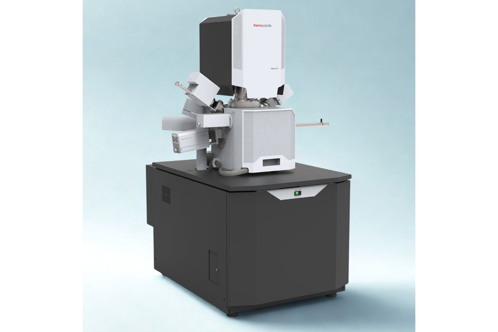
Thermo Fisher Apreo 2C FE-SEM — Field Emission SEM with nm-level resolution, EDS & EBSD

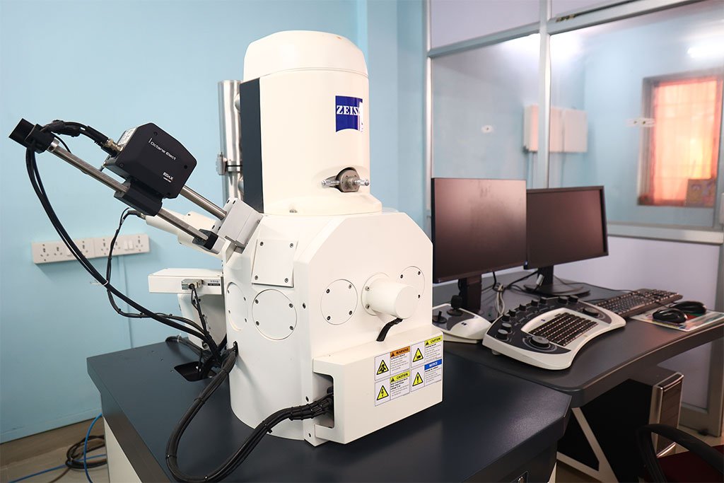
Zeiss SEM with EDAX Octane Elect EDS — high-resolution imaging and elemental analysis
Aerospace Materials Testing
Composites · Aerospace Grade
NADCAP Pursuit. NABL Accredited.
Accreditation & Compliance
Ready to qualify your composite?
Typical turnaround · 5–10 working days
FE-SEM Imaging
What Our Electron Microscope Reveals
01
Fracture Surface Studies
Identify fracture type — ductile (dimple rupture), brittle (cleavage), fatigue (striations), intergranular, mixed-mode. Beach marks, ratchet marks, fatigue origin identification.
02
Failure Analysis
Detect voids, inclusions, cracks, and surface defects at magnifications revealing details invisible to optical microscopy.
03
Material Characterization
Powder morphology, fiber analysis, coating cross-sections. Critical for additive manufacturing, composites, and surface engineering.
04
Contamination & Weld Analysis
Foreign particle identification with EDS chemical fingerprinting. Weld evaluation and heat-affected zone (HAZ) characterization.
EDS — Energy Dispersive X-ray Spectroscopy
- Elemental composition analysis at micro-scale
- Elemental mapping — spatial distribution across sample surface
- Line scans for compositional gradients across interfaces, coatings, and diffusion zones
- Inclusion & precipitate chemical identification
- Corrosion product and deposit analysis
EBSD — Electron Backscatter Diffraction
Crystallographic Analysis That Most Labs Can't Offer
EBSD provides spatially resolved crystallographic information — grain orientation, grain boundary character, phase distribution, and deformation analysis — essential for R&D, failure investigation, and advanced alloy development.
Inverse Pole Figure (IPF) Maps
Colour-coded crystallographic orientation maps revealing grain structure and preferred orientation.
Grain Size Distribution
Statistical analysis of grain diameters — number-weighted and area-weighted averages from sub-micron to tens of microns.
Misorientation Angle Distribution
Characterization of grain boundary types — low-angle vs. high-angle boundaries for understanding material behaviour.
Grain Boundary Maps
Visualization of boundary network with misorientation classification for understanding intergranular phenomena.
Phase Identification Maps
Multi-phase mapping for duplex, austenitic-ferritic, and multi-phase microstructures.
KAM & Texture Analysis
Local misorientation (KAM) maps for residual strain. Pole figures and ODF for texture quantification.
EBSD Analysis Data Output
| Parameter | Typical Range | Significance |
|---|---|---|
| Grain Size (Number Avg.) | 0.24 – 1.33 μm | Sub-micron to fine-grained |
| Grain Size (Area Avg.) | 2.85 – 7.43 μm | Area-weighted distribution |
| Misorientation (Avg.) | 16.6° – 25.9° | Low-angle to high-angle ratio |
| Magnification Range | 300x – 3000x+ | Multi-scale analysis |
EBSD Results Gallery

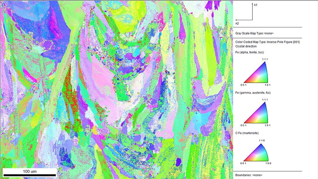
EBSD IPF Map — Additive Manufacturing (ferrite + austenite + martensite)

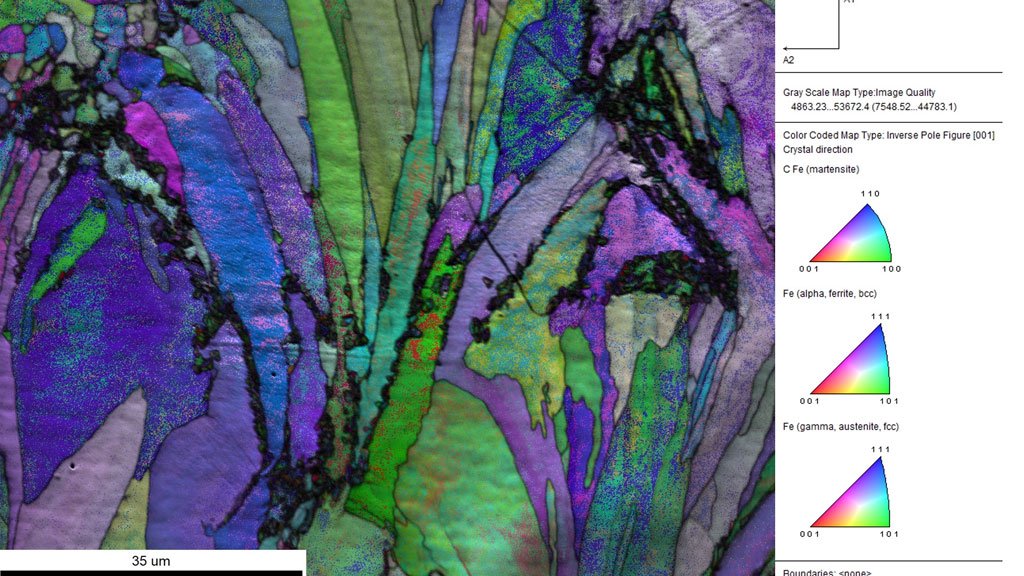
EBSD IPF Map — Martensite crystallography at 35 µm

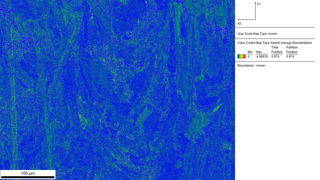
Kernel Average Misorientation (KAM) Map — strain localisation

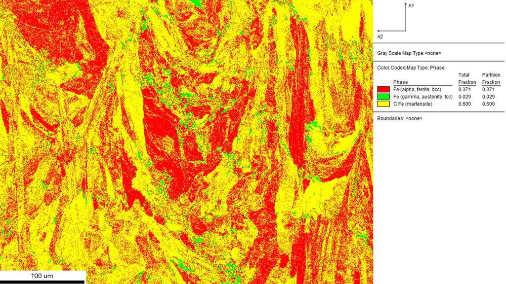
Phase Map — Ferrite (yellow), Martensite (red), Austenite (green)
EBSD Applications for R&D
Where EBSD Changes the Analysis
Weld Zone Characterization
Base metal, HAZ, and weld metal grain structure comparison — critical for understanding weld performance and qualification.
Recrystallization Studies
Grain growth after thermo-mechanical processing — validate heat treatment and forming parameters.
Additive Manufacturing
Columnar vs. equiaxed grain structure mapping — essential for AM process development and qualification.
Advanced Alloy Development
Superalloy and high-performance alloy texture and phase analysis for material development programs.
Deformation & Strain Analysis
Local misorientation (KAM) mapping for residual strain and deformation analysis in service-exposed components — correlating microstructural changes to failure mechanisms.
SEM Sample Work
Representative Imaging Results
A selection of SEM micrographs illustrating the range of materials and failure modes characterised at Microlab Testing.

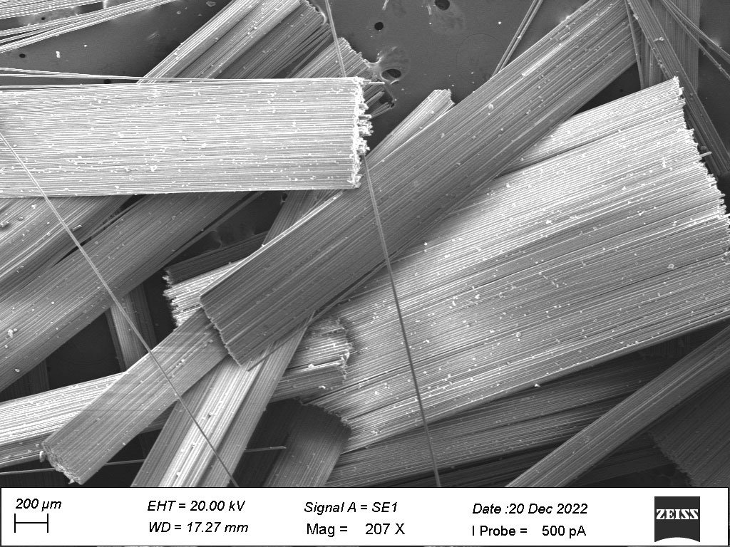
Fiber bundle morphology — 207x magnification

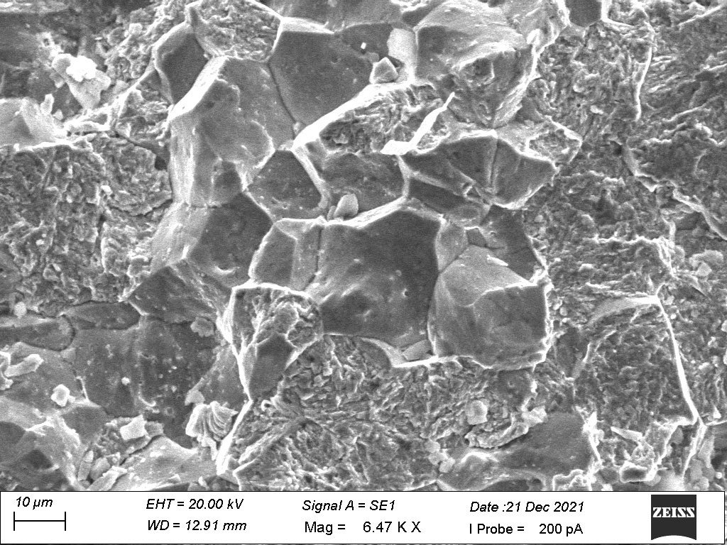
Intergranular fracture surface — 6470x

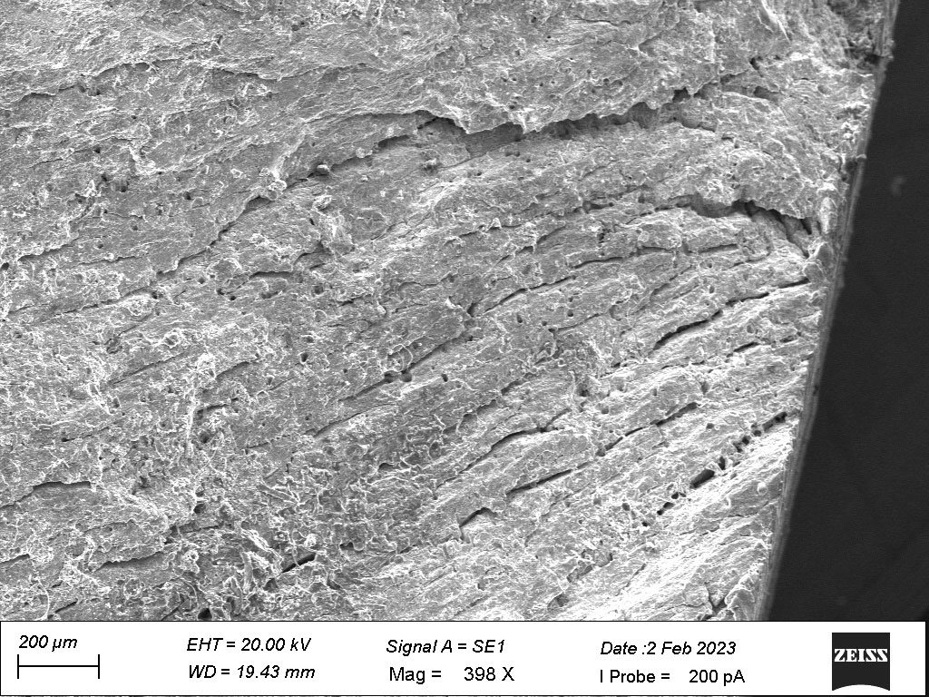
Longitudinal cracking in multilayer material — 308x

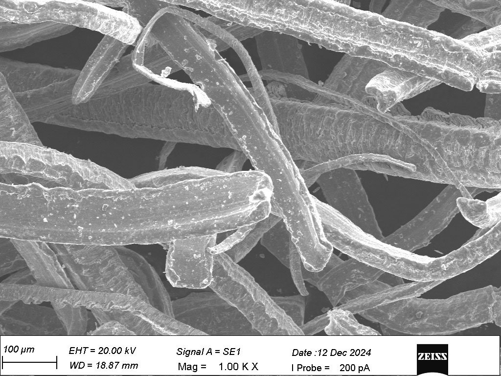
Metal fiber morphology — 1000x
Instrument Specifications
Measurable capabilities of our electron microscopy suite
| Parameter | Thermo Fisher FE-SEM | Zeiss SEM |
|---|---|---|
| Accelerating Voltage | 0.2 – 30 kV | 0.1 – 30 kV |
| Resolution | < 1 nm at 15 kV | < 1.5 nm at 15 kV |
| Detectors | SE, BSE, EDS (Silicon Drift), EBSD | SE, BSE, EDS |
| EDS Capability | Elemental mapping, point analysis, line scans, light-element detection (B, C, N, O) | Elemental mapping, point analysis, line scans |
| EBSD | Phase mapping, IPF orientation, KAM strain, grain-size distribution, misorientation analysis | N/A |
| Stage Capacity | Up to 150 mm diameter specimen | Up to 100 mm diameter specimen |
| Chamber Vacuum | High vacuum & low vacuum modes | High vacuum mode |
| Magnification | 25× to 1,000,000× | 20× to 500,000× |
Problem → Method Selection
Which SEM technique answers your engineering question
Fracture Origin Identification
SE imaging at fracture surface
Secondary electron fractography reveals initiation sites, beach marks, striations, cleavage facets, dimpled rupture, and intergranular separation — essential for failure analysis root-cause determination.
Contamination / Foreign Material
EDS elemental analysis
Point analysis and elemental mapping identify contaminant composition — corrosion products, inclusions, surface deposits, welding defects. Light-element detection (B, C, N, O) for interstitial contamination.
Inclusion Analysis
BSE imaging + EDS mapping
Backscatter electron imaging for atomic-number contrast reveals inclusions, precipitates, and second phases. Combined EDS confirms inclusion type (oxide, sulfide, silicate, nitride).
Coating / Layer Analysis
Cross-section BSE + EDS line scan
Coating thickness measurement, layer composition, interdiffusion zone analysis, porosity assessment, and substrate-coating interface evaluation for plated, PVD, CVD, and thermal-spray coatings.
Phase Identification
EBSD phase mapping
Crystallographic phase mapping distinguishes ferrite/austenite/martensite, alpha/beta titanium, gamma/gamma-prime in superalloys. Quantitative phase fractions with spatial distribution.
Grain Orientation & Texture
EBSD IPF + pole figures
Inverse pole figure (IPF) maps, pole figures, and orientation distribution functions for texture analysis in rolled, forged, and additively manufactured components. Critical for anisotropy assessment.
Deliverables & Output Types
What our SEM/EDS/EBSD reports include
SEM Imaging
High-resolution SE and BSE micrographs at multiple magnifications, annotated fracture surface maps, topographic and compositional contrast images, measurement overlays.
EDS Analysis
Elemental spectra, quantitative composition tables, elemental distribution maps (false-colour), line-scan profiles across interfaces/gradients, light-element detection results.
EBSD Maps
IPF orientation maps, phase distribution maps, kernel average misorientation (KAM) strain maps, grain boundary character distribution, grain-size statistics (ASTM E2627), pole figures and ODF plots.
Interpretation Report
Engineer-authored narrative linking observations to engineering context — failure mechanism identification, microstructural anomaly assessment, comparison with specification requirements, recommendations.
Sample Preparation Requirements
- Fracture surfaces: Do not clean, touch, or coat the fracture face. Protect with tissue and ship in rigid packaging. Avoid plastic bags (static charge attracts debris).
- Mounted/polished specimens: Final polish to 0.05 μm colloidal silica for EBSD. Standard metallographic polish for SEM imaging and EDS.
- Bulk samples: Max stage capacity 150 mm diameter. Irregular shapes can be sectioned and mounted in-house.
- EBSD specimens: Require vibratory polish or ion-beam finish for pattern quality. We handle this in-house if raw material is provided.
- Turnaround: Standard 5–7 working days. Express 2–3 days available for fractography and EDS. EBSD mapping typically 7–10 days.
2–4 Days
Standard Turnaround
1–2 Days
Express Available
ISO 17025:2017
Reports Expert Interpretations
Related Services
Metallography & Failure Analysis
Microstructure examination, root cause failure analysis, and fractography
Fatigue & Fracture
KIC, JIC, CTOD, da/dN, LCF/HCF fatigue and creep rupture testing
Corrosion Testing
SSCC, HIC, IGC, salt spray, pitting, and electrochemical corrosion evaluation
Metals Testing
Mechanical, chemical, and metallographic testing of ferrous and non-ferrous metals
Need SEM/EBSD Analysis for Your Materials?
Discuss your characterization requirements with our materials scientist. From fractography to crystallographic mapping.